Lab 1 Report
Introduction
In this lab, a design was implemented on the FPGA to program a seven segment display, from 0 to F given a binary input. LEDs were also programmed with set logic given the input, one LED was programmed to blink at 2.4 Hz.
Design and Testing Methodology
Design Overview
The first step in the design was to determine the logic needed for the LEDs which resulted in an XOR, AND gates. The blinking LED used the on-board high-speed oscillator to generate a 48 MHz clock signal, then a counter was used at a cycle of 10000000 to generate a 2.4 Hz blinking frequency. The second part of the design included the 7 segment display module that mapped the binary input to the neccesary segments that need to be turned on to the display the digit.
Testing Procedure
The design was tested using automatic testbenches in Questa. Testbenches were written for both the top module and the 7 segment display module. Testvectors with inputs and expected output values were given to compare the program outputs to the expected outputs. The waveforms were generated and compared to show that all 16 input values matches the segment display and led expectations. These simulations confirmed the physical behavior expected from the board.
Technical Documentation
Source Code
Block diagram
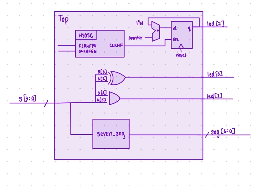
The block diagram in Figure 1 demonstrates the overall architecture of the design. The top module includes the led controls utilizing the HSOSC built in module for the clk. The submodule seven_seg handles the seven segment display outputs.
Schematics
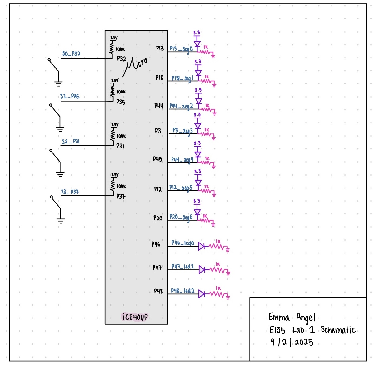 Figure 2 shows the physical layout of the design with the 4 input switches on the left and on the right the 7 segment LEDS along with the 3 external LEDs. For all LEDs a 1k ohm resistor was used to limit current draw. The input swithes were all configured with 100k ohm internal pullup resistors.
Calculation for current draw
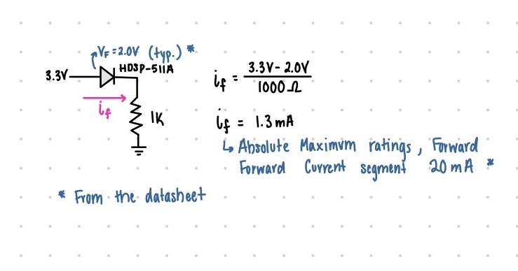
Figure 3 shows the current draw calculation for each seven segment LED display. Using the forward voltage from the data sheet and a standard 1k ohm resistor we can solve for the current through the LED which comes out to 1.3 mA. This current is pretty standard for an LED and is well under the absolute maximum forward current of 20 mA (from the datasheet).
Results and Discussion
Testbench Simulation
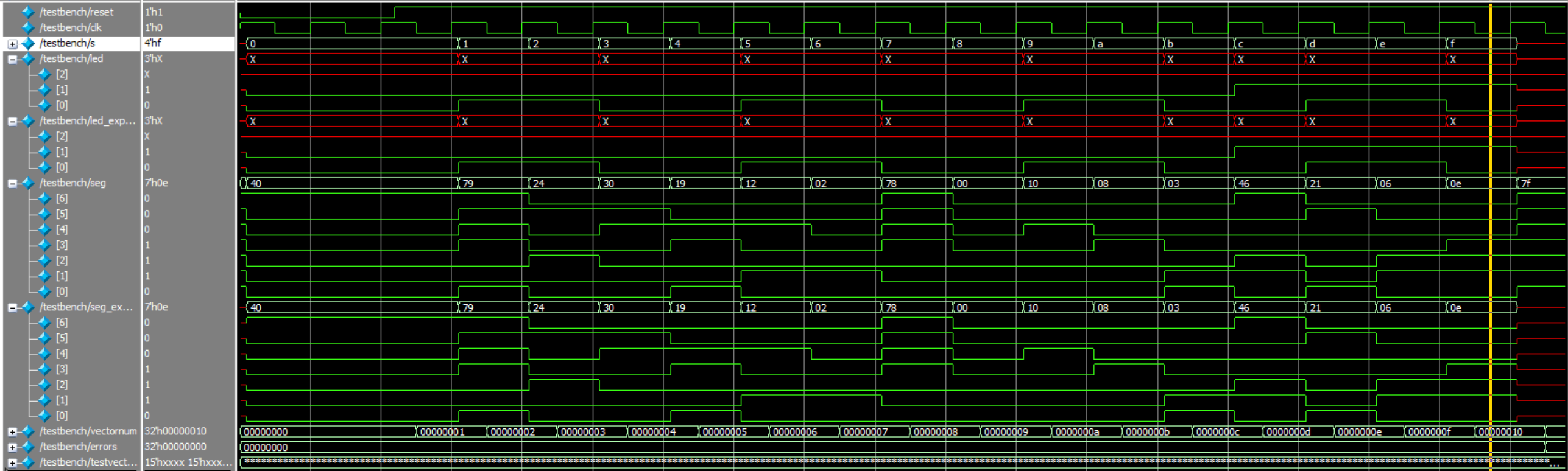
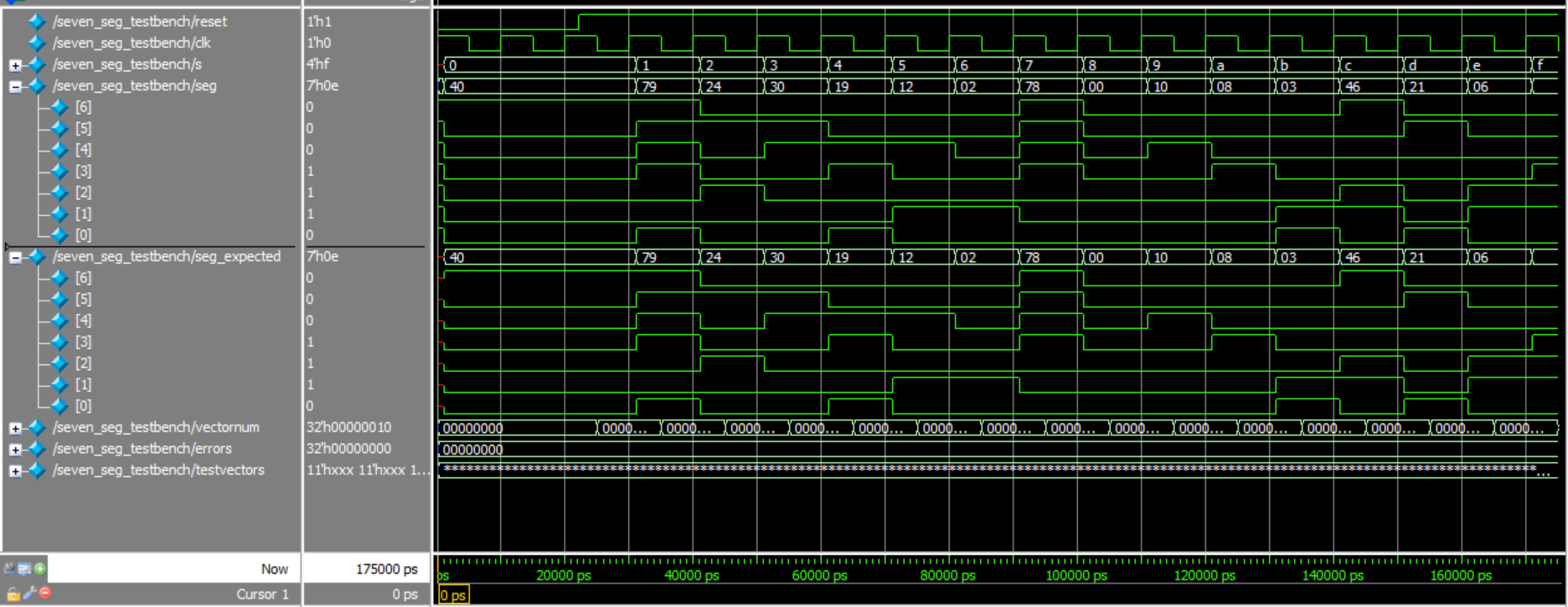
The design met all the objectives. Shown are the QuestaSim simulations for both the top module and the seven segment module. The outputs and the expected outputs can be compared for both modules showing that all 16 inputs matched the expected outputs.
Conclusion
The design was succesful with the seven segment display showing the correct hex numbers. The LEDs demonstrated the correct logic and the correct blinking frequency of 2.4 Hz. From start to finish I spent ~25 hours working on this lab.
AI Prototype Summary
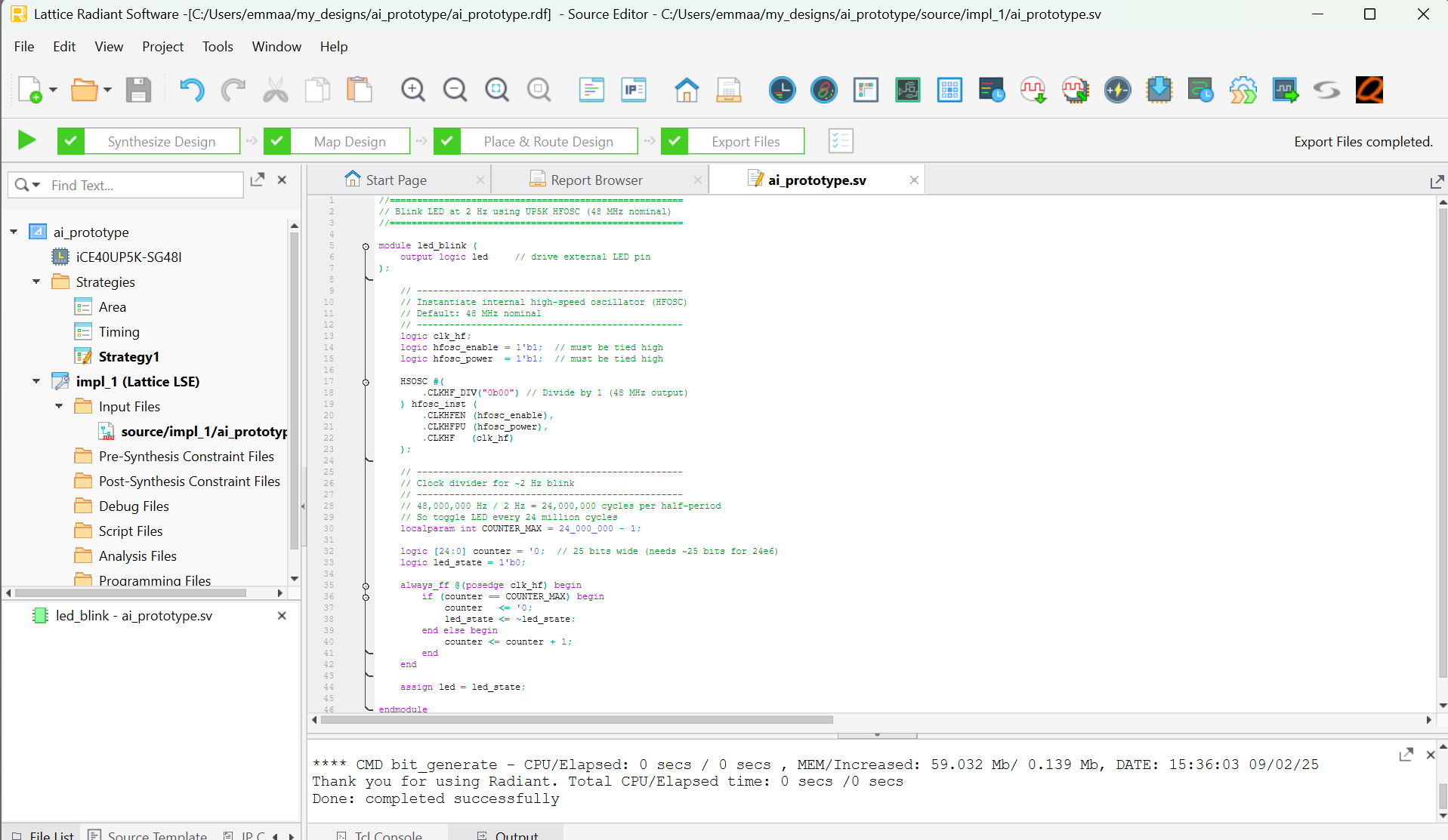
I gave the prompt to chatGPT and then I ran the code in raiant and the code synthesized just fine the first time. Above is screenshot showing the synthesized code.
Just looking at how the ai solved the problem I can see that it seemed to define variables when maybe they weren’t really needed. However, the ouput seems right it does seem to produce the correct blinking. The LLM used localparam int which is a new variable type or at least one I haven’t seen used a lot. Althought the LLM synthesized I have a feeling there would be issues either simulating the code or testing it in hardware since that was still true for my own code. I think using AI at the end shows you that the logic and structure I used was correct and pretty standard however you need to work through it on your own in order to trust what the LLM is producing.