Lab 2 Report
Introduction
In this lab, a design was implemented on the FPGA to program a two seven segment displays from 0 to F using a single seven segment module given a two 4 bit binary inputs. Five external green LEDs were programmed to display to the sum of the two digits displayed.
Design and Testing Methodology
Design Overview
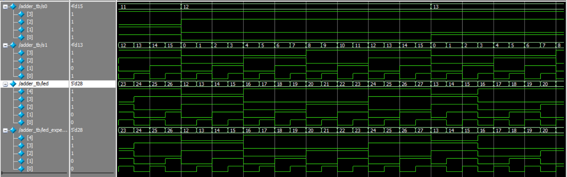
The first step in the design was to determine the overall structure needed and the number of modules needed. The main function of this design was the flicker module which controlled the the oscillating signals that would control one segment at a time. The on-board high-speed oscillator was used to generate a 12 MHz clk signal that was fed into the flicker module. A 24 bit counter was used and on the 16th bit the counter would reset. The module would also need to output the 4 bit s value that corresponding to the current display being turned on. This s value that was to be displayed is fed into the seven segment module that outputs the correspdning segment values needed to display that digit. Lastly, a simple adder module was implemented to output the 5 bit sum or the two 4 bit inputs.
Testing Procedure
The design was tested using automatic testbenches in Questa. Testbenches were written for each module: top, adder, flicker and the 7 segment display module. For the seven segment display testvectors were used same as in lab 1. The rest of the modules used assert statement within the testbench. The adder and flicker loop through all 256 cases for the two 4 bit input. The adder module asserted that the addition was correct. The flicker module checked that the cur_s output matched the corresponding anode0/anode1 signal. The top module asserted that the current signal high (anode0/anode1) matched the outputed segment values. For the top moduel expected values were generated for the led expected values and the segment expected values. The waveforms were generated and compared to confirm the behavior of the modules. These simulations confirmed the hardware behavior expected from the board.
Technical Documentation
Source Code
Block diagram
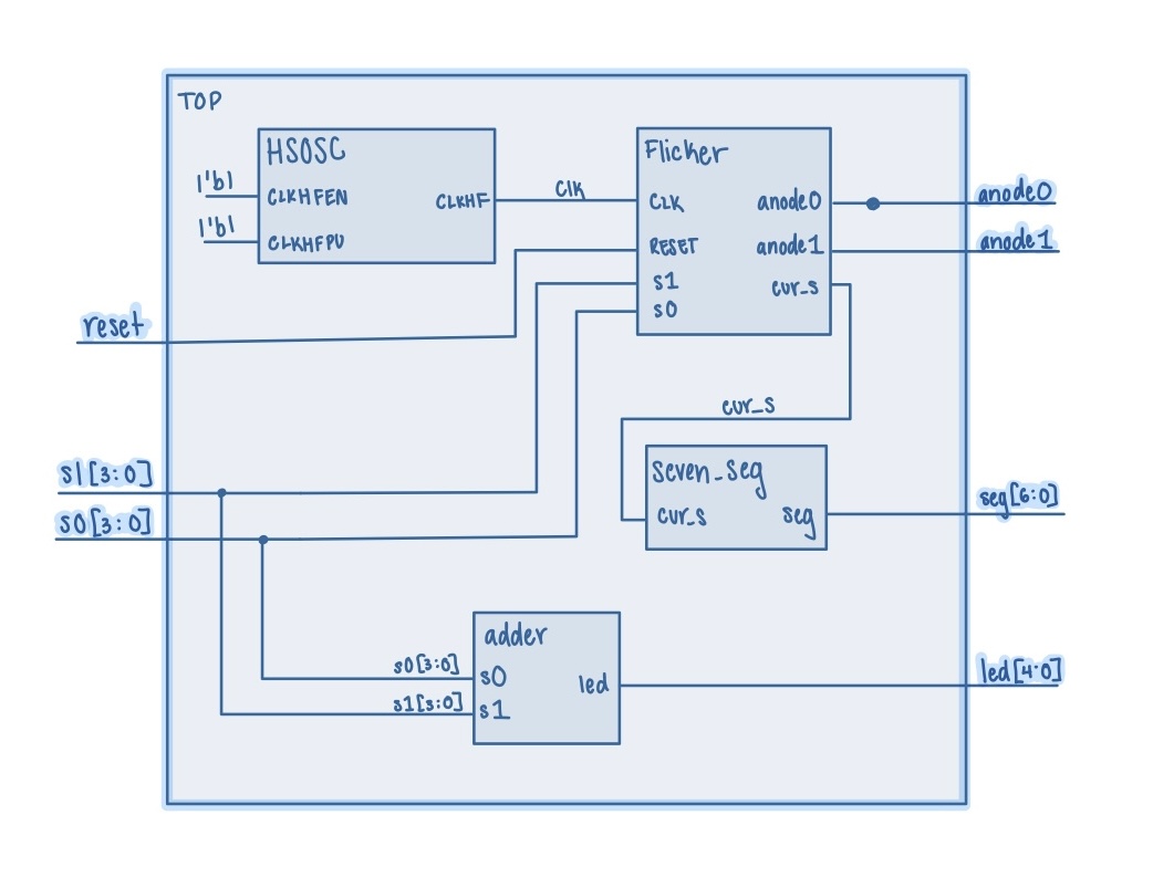
The block diagram in Figure 1 demonstrates the overall architecture of the design. The top module utilizes the HSOSC built in module for the clk. The submodule seven_seg handles the seven segment display outputs. The submodule adder handles the addition of s0 and s1 for the led output and the submodule flicker handles the alternating flickering signals and outputting the correct s value to be displayed at a given time.
Schematics
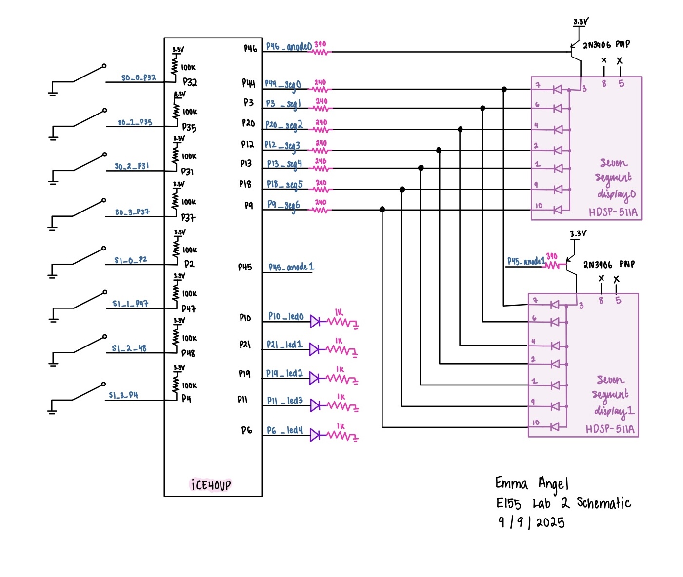 Figure 2 shows the physical layout of the design with the 8 input switches on the left and on the right the two seven segment displays sharing the same output pins alone with 5 external green LEDs. For the green LEDs a 1k ohm resistor was used to limit current draw. The seven segment displays used a 240 ohm resistor. The transistor was used to drive a large amount of current for the anode pins of the display and a 390 ohm resistor was used to limit current draw from the FPGA pin.
Calculation for current draw
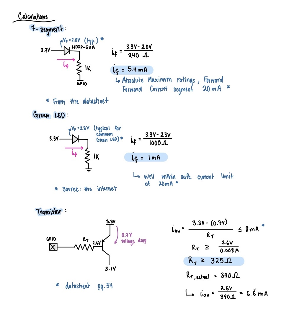
Figure 3 shows the current draw calculation for the seven segment LED display, green LEDs, and transistor circuit. For the seven segment display, using the forward voltage from the data sheet and a 240 ohm resistor we can solve for the current through the LED which comes out to 5.4 mA. This current is pretty standard for an LED and is well under the absolute maximum forward current of 20 mA (from the datasheet).For the green LEDs the same calculation was used this time with a 1k ohm resistor to limit current down to 1 mA which is a very safe current for standard LEDs. For the transistor, we can take the difference of voltage from the 3.3V source and the 0.7V drop from the source to the gate and divide by R_t. The maximum output current from the FPGA pin is 8 mA per the datasheet. Solving the inequality results in the resisotr value must be greater than 325 ohms.
Results and Discussion
Testbench Simulation
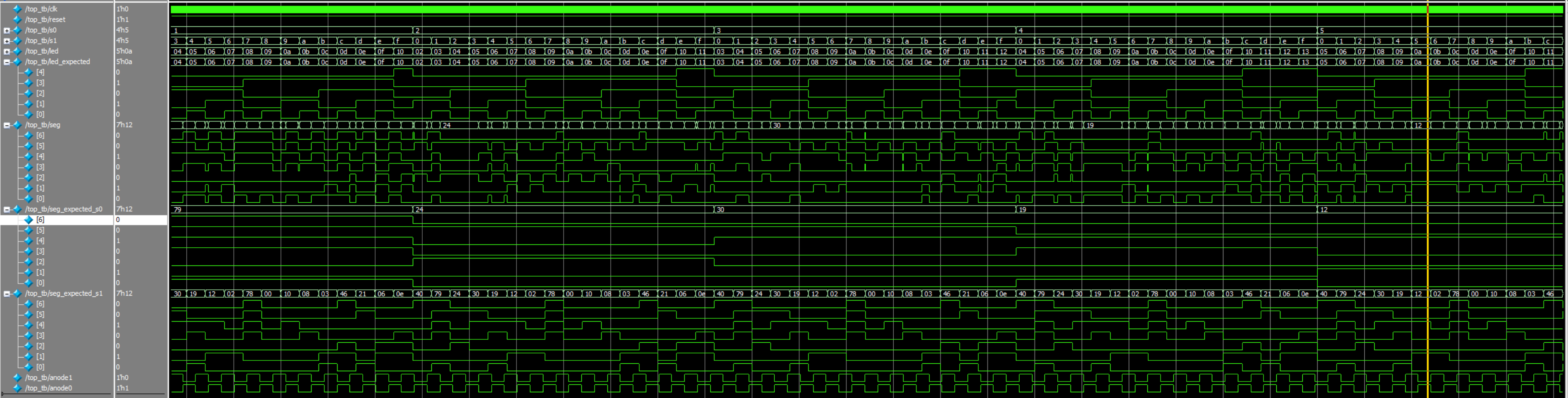 Top module testbench shows a more zoomed out version of all the signals.
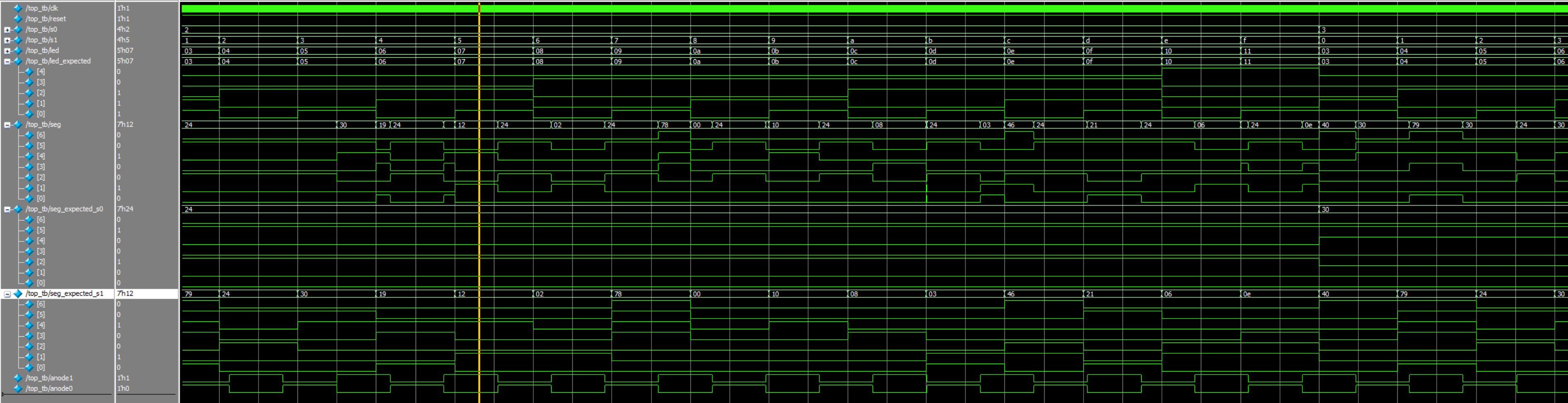 Shows a zoomed version a couple of specific test cases to better see the outputs.
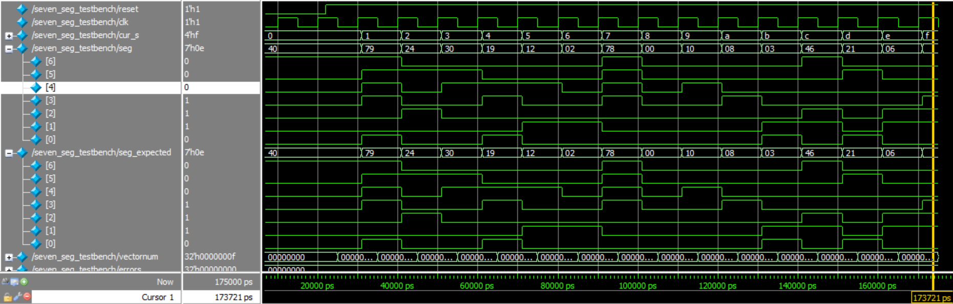 Seven segment tesbench that is the same as lab 1. I reran the testbench to show it worked within this module but code remained the same.
 This is zoomed in so that you can see the actual values being outputed but all 256 cases were tested.
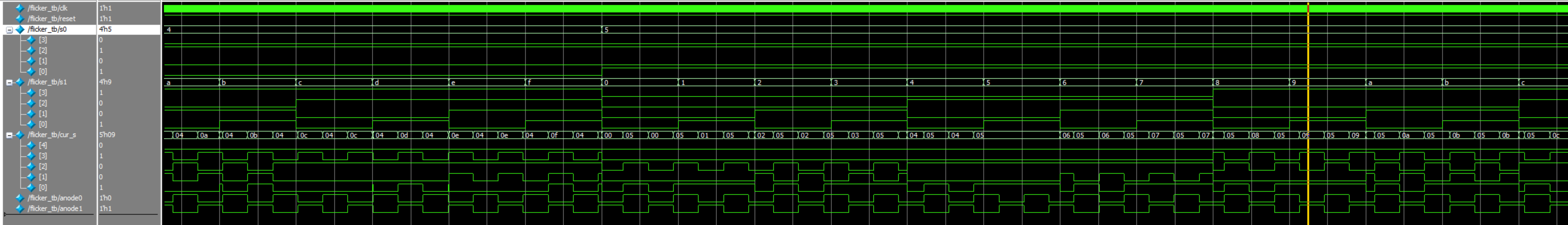 This is the flicker module test bench that shows that the cur_s value matches the right input s0 or s1 based on which anode0/anode1 signal is high.
The design met all the objectives. Shown are the QuestaSim simulations all the submodules and the top module. The outputs and the expected outputs can be compared showing that all 256 inputs matched the expected outputs.
Conclusion
The design was successful with the two seven segment displays showing the correct hex number without visible flickering or bleeding of the digits. Only one seven segment module was used. The green LEDs display the the sum of the two 4 bit binary inputs. I spent ~20 hours working on this lab.
AI Prototype Summary
Code produced by chatGPT from the first prompt.
// -----------------------------------------------------------------------------
// seven_seg_decoder_ca
//   4-bit hex to 7-seg decoder for a *common-anode* display.
//   Segment order is {a,b,c,d,e,f,g}; active-low outputs (0 lights a segment).
// -----------------------------------------------------------------------------
module seven_seg_decoder_ca (
    input  logic [3:0] nibble,
    output logic [6:0] seg   // {a,b,c,d,e,f,g}, 0 = on
);
    always_comb begin
        unique case (nibble)
            4'h0: seg = 7'b0000001; // 0
            4'h1: seg = 7'b1001111; // 1
            4'h2: seg = 7'b0010010; // 2
            4'h3: seg = 7'b0000110; // 3
            4'h4: seg = 7'b1001100; // 4
            4'h5: seg = 7'b0100100; // 5
            4'h6: seg = 7'b0100000; // 6
            4'h7: seg = 7'b0001111; // 7
            4'h8: seg = 7'b0000000; // 8
            4'h9: seg = 7'b0000100; // 9
            4'hA: seg = 7'b0001000; // A
            4'hB: seg = 7'b1100000; // b
            4'hC: seg = 7'b0110001; // C
            4'hD: seg = 7'b1000010; // d
            4'hE: seg = 7'b0110000; // E
            4'hF: seg = 7'b0111000; // F
            default: seg = 7'b1111111; // all off
        endcase
    end
endmodule

// -----------------------------------------------------------------------------
// two_digit_time_mux
//   Time-multiplex one decoder instance across two 4-bit inputs.
//   The single decoder's output is latched alternately into seg0 and seg1.
//   Parameterizable scan rate via a simple clock divider.
// -----------------------------------------------------------------------------
module two_digit_time_mux #(
    // Divide ratio for the scan tick. With a 50 MHz clock, DIV_POW2=15 -> ~1.5 kHz toggle
    // (per digit ~750 Hz refresh), which is flicker-free. Adjust for your clock.
    parameter int unsigned DIV_POW2 = 15
) (
    input  logic        clk,
    input  logic        rst_n,      // active-low synchronous reset

    input  logic [3:0]  in0,        // 4-bit value for "digit 0"
    input  logic [3:0]  in1,        // 4-bit value for "digit 1"

    output logic [6:0]  seg0,       // latched segments for digit 0 (active-low)
    output logic [6:0]  seg1        // latched segments for digit 1 (active-low)
);
    // Clock divider to create a scan "tick"
    logic [DIV_POW2-1:0] div_cnt;
    logic                scan_tick;

    always_ff @(posedge clk) begin
        if (!rst_n) begin
            div_cnt   <= '0;
            scan_tick <= 1'b0;
        end else begin
            div_cnt   <= div_cnt + 1'b1;
            scan_tick <= (&div_cnt); // tick when counter rolls over
        end
    end

    // Which input are we currently decoding?
    logic select_digit;  // 0 -> in0/seg0, 1 -> in1/seg1
    always_ff @(posedge clk) begin
        if (!rst_n) select_digit <= 1'b0;
        else if (scan_tick) select_digit <= ~select_digit;
    end

    // Mux the current 4-bit input into the single decoder
    logic [3:0] current_nibble;
    always_comb begin
        current_nibble = (select_digit == 1'b0) ? in0 : in1;
    end

    // Single shared decoder
    logic [6:0] decoded_seg;
    seven_seg_decoder_ca u_dec (
        .nibble (current_nibble),
        .seg    (decoded_seg)
    );

    // Latch the decoder output into the correct digit on each scan tick
    always_ff @(posedge clk) begin
        if (!rst_n) begin
            seg0 <= 7'b1111111; // all off (common-anode)
            seg1 <= 7'b1111111;
        end else if (scan_tick) begin
            if (select_digit == 1'b0) seg0 <= decoded_seg;
            else                      seg1 <= decoded_seg;
        end
    end

endmodule
I gave the prompt to chatGPT and then I ran the code in raiant and the code synthesized just fine the first time. The methods used my chatGPT are kind of confusing to me and aren’t very readable. I took a lot at the netlist analyzer and I saw that its outputting seg0 and seg1 even though the top level module only outputs seg.
Next, I gave chatGPT my lab 1 files, at first it didn’t actually open the files instead it just assumed what was int he file based on the second prompt so I had to ask it to actually open the files. Looking at that code produced it was a lot more similar to how I approached lab 2 because it was based off lab 1. One thing I noticed is that it used two different latches for the counter behavior and for the mux behevior and in my code those two behaviors are in the same always_ff block. This second run the quality of the output appeared to be a lot better because it was something I could more easily understand and didn’t use any unknown syntax/constructs. This code also synthesized fine the first time around, however, I feel like synthesizing isn’t exactly the best measure for the quality of code since it likely won’t do the intended behavior. I’m noticing that the LLMs don’t really like making new modules unless they are directed to so thats a design decision that it doesn’t execute very well. Giving the LLM files of my own code that were similar makes its a lot easier to understand the output code and trust that the module is having the intended behavior.